
In the semiconductor industry, where a single micron can be the difference between a high-yield batch and a costly failure, the choice of metrology material is critical. As lithography and wafer inspection push the boundaries of physics, traditional metal and even high-grade granite are reaching their limits.
Alumina Ceramic (Al2O3) has emerged as the definitive solution for semiconductor equipment manufacturers. With a precision retention span that can exceed traditional materials by over 10 years, ceramics are no longer a luxury—they are a structural necessity.
Why Alumina Ceramic for Semiconductors?
Before diving into applications, it is essential to understand the material’s unique “triple-threat” profile:
-
Thermal Stability: A low coefficient of thermal expansion (≈7 × 10^{-6}/K) ensures measurements remain consistent despite heat generated by high-speed equipment.
-
Non-Magnetic & Non-Conductive: Essential for vacuum environments and sensitive electron-beam lithography where magnetic interference can deflect beams.
-
Zero Corrosion: Unlike steel, ceramics are chemically inert, making them compatible with cleanroom cleaning protocols and corrosive gas environments.
5 Key Applications in Semiconductor Equipment
1. Lithography Machine Stages
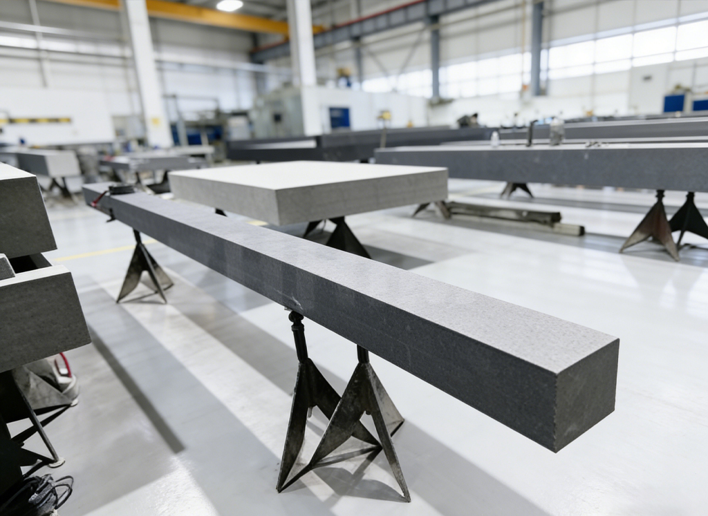
Modern photolithography requires nanometer-level positioning. Ceramic squares and structural components serve as the “master reference” for the wafer stage. Their high stiffness-to-weight ratio allows for rapid acceleration without the vibration or “ringing” associated with heavier materials.
2. Wafer Inspection & Metrology
In wafer geometry systems, Ceramic Master Squares are used to calibrate the perpendicularity and straightness of the scanning axes. Because ceramic maintains its shape over a decade, these machines require far fewer recalibration cycles, maximizing uptime for the fab.
3. Precision Assembly of Vacuum Chambers
Semiconductor assembly often happens in vacuum environments where lubrication is limited. Ceramic gages provide a “dry” precision reference that won’t outgas or contaminate the vacuum, ensuring that internal components are aligned to sub-micron tolerances.
4. High-Frequency Electronic Testing
For high-speed chip testing, any magnetic or conductive interference from the measuring tool can skew results. Alumina ceramic’s non-magnetic nature makes it the ideal material for probe card fixtures and alignment gages.
5. Cleanroom Calibration Masters
In ISO Class 1 cleanrooms, rust is a forbidden contaminant. Steel gages require oil films to prevent oxidation, which is a major contamination risk. Ceramic gages require no oil and can be cleaned with isopropyl alcohol, maintaining a “zero-particle” profile for 10+ years.
The “10-Year Advantage”
While metal gages may warp or wear after a few years of intensive use, the molecular structure of high-purity Alumina is incredibly stable. When used as a Ceramic Square or Straight Edge, the material’s hardness (approaching that of sapphire) prevents the microscopic surface degradation that typically causes accuracy to “drift” over time.
For a semiconductor OEM, this means a 10-fold reduction in long-term maintenance costs and a significantly higher level of trust in the machine’s lifetime accuracy.
Post time: Mar-23-2026