
1. Structural Pain Points of Traditional Frames in Semiconductor Inspection
Semiconductor components feature micro and nano-scale precision. Tiny frame fluctuations will be greatly amplified by high-sensitivity inspection systems, resulting in misjudged defects, dimensional errors and poor data repeatability. Traditional metal gantries have three typical drawbacks. First, metal structures are magnetizable and easily interfere with optical sensors, laser modules and encoders, affecting weak signal acquisition. Second, general structural rigidity cannot support high-frequency micro-scanning and precise positioning, causing micro-tremor and deflection deformation. Third, metal surfaces oxidize and peel off easily, producing fine particles that fail strict semiconductor cleanroom standards.
In addition, different semiconductor inspection equipment varies greatly in stroke, load, installation interface and motion logic. Standard universal gantries cannot match personalized assembly requirements, easily leading to benchmark misalignment and insufficient structural performance. This makes customized gantry structures essential for high-end semiconductor inspection machines.
2. Application-Tailored Custom Design for Full Semiconductor Scenarios
ZHHIMG semiconductor-dedicated granite gantries abandon universal design modes and adopt one-to-one customized development according to actual equipment parameters and working conditions. For large-stroke wafer scanning equipment, we optimize beam span and bending resistance to improve overall motion stability. For high-frequency micro-defect detection devices, local structural rigidity is strengthened to eliminate tiny vibration-induced inspection errors.
All guide rail grooves, grating datum surfaces, motor mounting positions and fixture positioning holes are integrally precision-machined according to original equipment parameters, requiring no secondary modification and avoiding stress deformation. Integral or split structures with special sizes are available to adapt to different cleanroom layouts and equipment forms, balancing compact installation space and ultra-precision operation performance.
3. High-Rigidity Stone Material for Micro-Nano Inspection Accuracy
Adopting high-purity dense black granite exclusively selected through strict mineral screening, the material features uniform crystal distribution, ultra-high compression rigidity and superior structural stability compared with ordinary stone and metal. Through long-term static aging and multi-stage stress relief, the blank completely eliminates residual processing stress, ensuring no plastic deformation or elastic fatigue under long-term dynamic load.
Optimized thickened beam and symmetrical column structure greatly enhance bending, torsion and compression resistance. The rigid frame effectively counteracts dynamic stress generated by high-frequency scanning and frequent start-stop movement, maintaining stable geometric tolerance and benchmark flatness. It fundamentally avoids accuracy drift, micro-deformation, misdetection and missed detection in long-term semiconductor inspection operations.
4. Semiconductor-Grade Properties for Strict Advanced Process Standards
Different from ordinary industrial gantries, semiconductor-specific granite structures own two key advantages for cleanroom environments. Firstly,non-magnetic and insulating performance ensures zero electromagnetic interference with laser imaging, optical detection and precision sensing systems, enabling accurate weak signal capture. Secondly, the dense pore-free stone surface is anti-corrosive, dust-proof and oil-resistant. After ultra-fine mirror polishing, the surface never peels or produces micro-particles, fully complying with semiconductor cleanliness specifications.
With ultra-low thermal expansion coefficient, the granite frame remains dimensionally stable under slight temperature and humidity fluctuations, maintaining consistent ultra-precision benchmarks for wafer, chip and packaging component inspection in constant-temperature semiconductor production lines. 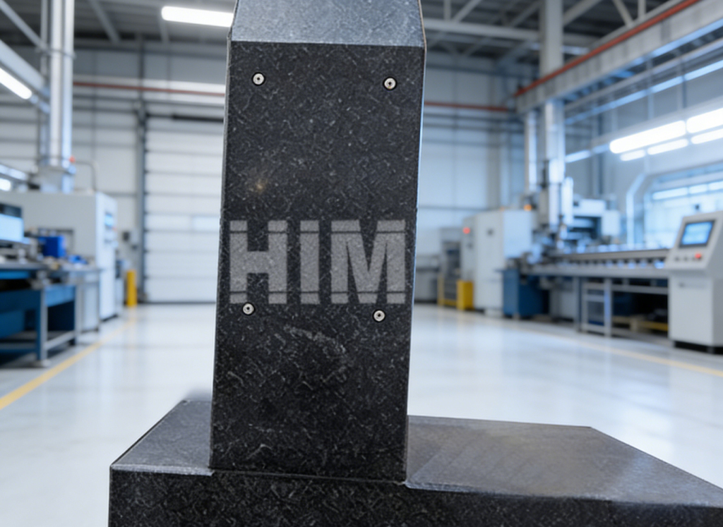
5. Constant-Temperature Precision Manufacturing Ensures Long-Term Stability
All customized semiconductor gantries are processed, lapped and calibrated in constant-temperature, humidity-controlled, dust-free and vibration-isolated workshops. Equipped with imported high-precision measuring instruments, we conduct full-range nanometer-level calibration for flatness, straightness, perpendicularity and parallelism, providing fully traceable test data that meets advanced semiconductor manufacturing standards.
All splicing and mounting surfaces adopt high-precision manual lapping to achieve gap-free fitting and zero benchmark deviation. It ensures accurate assembly and smooth operation of transmission and detection modules. The gantry system requires minimal routine calibration, maintaining ultra-precision performance for long-term mass production and effectively improving semiconductor inspection efficiency and product yield.
Conclusion
The accuracy limit of semiconductor inspection equipment depends on the adaptability and stability of the structural benchmark. Universal frames can no longer meet micro-nano level process requirements. ZHHIMG custom high-rigidity granite gantry structures solve typical industry pain points including electromagnetic interference, micro-vibration, precision drift and insufficient cleanliness. With professional semiconductor scenario customization, high anti-deformation rigidity, zero-interference clean performance and strict quality control, ZHHIMG provides long-term stable precision benchmark solutions for wafer testing, chip screening and packaging inspection equipment, empowering quality upgrading in semiconductor precision manufacturing.
Post time: Aug-25-2026