
Modern semiconductor manufacturing operates at a scale of complexity that is difficult to overstate. A leading-edge logic chip contains transistors with gate lengths measured in a few nanometers — smaller than the width of a strand of DNA. Printing these features onto a silicon wafer requires positioning accuracy that makes even the most precise mechanical engineering of previous industrial eras look coarse by comparison. Yet at the foundation of this nanoscale process — often quite literally — sits a precisely machined block of igneous rock.
Granite structural components are ubiquitous in semiconductor capital equipment, and understanding why requires looking at the full system-level engineering of these machines: what errors need to be controlled, how they propagate through the system, and what material properties make granite uniquely well-suited to the role it plays.
The Semiconductor Equipment Error Budget: Understanding the Stack
Every precision positioning system — and semiconductor processing equipment is essentially a collection of extremely precise positioning systems — operates against what engineers call an error budget. The total allowable positioning error is distributed across all the sources of error in the system: encoder resolution, bearing straightness, thermal drift, vibration, actuator nonlinearity, and structural deformation, among others.
In a photolithography scanner or step-and-scan system used for IC manufacturing, the total overlay error (the accuracy with which one printed layer aligns to the previous one) must be controlled to a fraction of the minimum feature size being printed. At 7nm process nodes, overlay requirements can be below 2nm. The contribution of the structural base to this error budget — through thermal drift, vibration coupling, or long-term dimensional instability — must be kept to a small fraction of this total.
This is not a constraint that can be met by using a different control algorithm or a faster sensor. It requires the structural material to be inherently stable. You cannot feedback-correct a drift that you cannot measure, and you cannot fully compensate for errors that occur at frequencies or length scales below your sensor’s resolution. This is why the choice of base material matters: it determines the fundamental floor below which active control cannot help.
Thermal Management: The Central Challenge
Of all the stability requirements imposed on structural components in semiconductor equipment, thermal management is typically the most demanding. Semiconductor processing environments are temperature-controlled with great care — cleanrooms for lithography are typically held to 20°C ± 0.01°C or even tighter in the exposure zone. But even with this level of environmental control, thermal gradients and temporal fluctuations impose constraints on equipment design.
Consider a granite gantry structure supporting a wafer stage in a photolithography system. If this structure experiences a temperature gradient of 0.01°C from one end to the other — already an extremely well-controlled condition — and it is 1 meter long with a CTE of 7 × 10⁻⁶/°C, the resulting differential expansion is approximately 70 picometers. At first glance, this seems negligibly small. But in the context of a 2nm overlay specification, this single thermal contribution already consumes 3.5% of the total error budget. Every other thermal source — motor heat, bearing friction, stage acceleration energy — competes for the remaining budget.
This is why thermal coefficient of expansion is not just a specification item for granite — it is a primary selection criterion. And it is why density matters in a way that is not immediately obvious: higher-density granite (such as premium black granite with density ≈ 3,100 kg/m³) has lower porosity, meaning less absorbed moisture and therefore less hygroscopic dimensional change as ambient humidity varies slightly. For semiconductor equipment, this distinction between premium and ordinary granite is not theoretical — it is measurable in the machine’s final performance.
Vibration Isolation and Damping: Protecting the Exposure Zone
Semiconductor equipment cleanrooms sit on isolated floor slabs designed to minimize the transmission of external vibrations. But even with active vibration isolation systems — air bearings, electromagnetic actuators, or inertial sensors feeding into active damping loops — the structural components of the equipment itself must not amplify or poorly attenuate the residual vibrations that reach them.
Granite’s damping coefficient (the rate at which mechanical vibration energy is absorbed and converted to heat within the material) is typically three to five times higher than that of cast iron and significantly higher than structural steel. For a component that forms a rigid mounting structure for sensitive optical elements or positioning stages, this difference in material damping can mean the difference between a vibration disturbance that decays within a few milliseconds and one that rings for tens of milliseconds — long enough to cause blur in an exposure, a positioning error in a wafer handler, or a measurement artifact in an in-line inspection system.
In practical equipment design, this manifests in how engineers specify structural elements. The mounting bridge of a wafer stage system, the column structure of a vertical inspection machine, the base plate of a projection lens assembly — all benefit from granite’s combination of high stiffness (high elastic modulus relative to its density) and high material damping. The combination gives a granite structure a relatively high natural frequency and rapid decay of forced oscillations, both desirable properties in precision positioning system design.
Long-Term Dimensional Stability: The Geometry of Trust
Semiconductor equipment is expensive — leading-edge lithography systems cost hundreds of millions of dollars — and it is expected to operate within specification for years or even decades. Within this service life, the dimensional relationships between key structural elements must remain stable to within the system’s error budget. Even slow drifts — on the timescale of months — can accumulate into alignment errors that degrade yield or force unscheduled recalibration.
This is where granite’s geological prehistory becomes a practical engineering advantage. Granite that has been quarried, stabilized, and processed has already undergone the stress-relief and consolidation processes that would otherwise cause dimensional drift in service. A well-processed granite structure does not creep under its own weight; it does not release residual machining stresses over months; it does not undergo phase changes or precipitation reactions that alter its volume. Within the operating range of temperatures and loads encountered in semiconductor equipment, a precision granite structure will maintain its geometry with a stability that no current structural metal can match over equivalent timescales without active thermal compensation.
This stability is not automatic — it depends critically on the quality of the raw material and the processing method. Stone that has been cut and processed too rapidly, without adequate stress-relief periods, may continue to drift after delivery. This is why reputable precision granite manufacturers include controlled aging periods in their production process, and why incoming material verification — checking density, hardness, and grain structure of each batch — is essential quality practice.
Specific Applications of Granite Components in Semiconductor Equipment
Wafer Stage Base Plates and Reference Surfaces
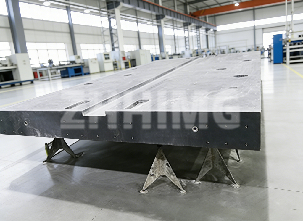
The stage that moves silicon wafers in a lithography system must position each die location within the beam of the exposure source with sub-nanometer repeatability. The base plate on which the stage guidance system is mounted — and the reference surface against which the stage position is measured by laser interferometry or linear encoders — must be flat, stable, and non-deforming.
Granite base plates for wafer stages are typically lapped to flatness values below 1 μm over the full stage travel range, and in some designs, to values in the hundreds of nanometers. The granite provides the physical reference against which all positioning measurements are made; any form error in this reference surface appears directly in the machine’s positioning accuracy.
Optical Column Structures and Lens Mounting Frames
The objective lens or projection lens assembly of a photolithography system must maintain precise alignment between lens elements to within a fraction of a wavelength of the illumination light. The structural frame mounting these lens elements must resist deformation from thermal loads, gravity, and dynamic forces during operation.
Granite structures are used in some system designs as mounting frames for projection optics, particularly in systems where long-term alignment stability is more critical than dynamic performance. The combination of high stiffness, low CTE, and zero magnetic permeability (which could otherwise affect magnetically-actuated lens elements) makes granite a competitive choice for these applications.
Metrology Frames in Process Equipment
In many semiconductor process tools — deposition systems, etch chambers, inspection machines — the actual processing environment is too aggressive (chemically or thermally) for a granite structure. But these tools still need a stable external reference frame against which process positions are measured. Granite metrology frames mounted outside the process chamber but connected to it through precision kinematic mounts serve this role, providing a thermally stable measurement reference that is isolated from the harsh process environment.
PCB Drilling Machines and Substrate Processing Equipment
Beyond silicon wafer processing, the broader electronics manufacturing ecosystem includes PCB drilling machines that create the via holes connecting layers in a multilayer circuit board, and substrate processing equipment for advanced packaging. These machines require base structures that maintain the positional relationship between multiple high-speed spindles to within tolerances of a few micrometers over thousands of hours of operation. Granite bases provide the required long-term stability against vibration coupling between spindles and against the thermal loading from high-speed drilling motors.
System-Level Design Considerations: Matching Granite to the Application
Not every application in semiconductor equipment calls for the same grade of precision granite. System designers working with granite structural components should consider several factors:
Form factor and weight — Granite’s density (2,700–3,100 kg/m³ depending on grade) makes large components heavy, and the support structure must be designed accordingly. Air bearing systems used to float heavy granite stages require careful calculation of load capacity and surface pressure.
Surface finish requirements — Air-bearing guide surfaces require extremely low roughness (Ra < 0.1 μm is typical) to function correctly. This places demands on the lapping process and on the hardness and grain structure of the stone.
Thermal management of the granite itself — For the most demanding applications, granite components may incorporate internal coolant channels (typically flowing temperature-controlled water) to actively control the temperature of the component and suppress thermal gradients. This requires careful design of the thermal interface between coolant channels and the surrounding stone, and precise temperature control of the coolant circuit.
Interface design — Granite is stiff and brittle; it cannot be clamped or bolted with the same freedom as metal without risk of cracking or introducing distortion. Kinematic mount designs — using three-point contact to constrain all six degrees of freedom without over-constraint — are standard practice for mounting precision granite components to their support structures.
The Relationship Between Base Stability and Yield
Semiconductor manufacturing yield — the fraction of chips on a wafer that meet specification — is sensitive to systematic spatial errors in the lithography process. An overlay error that is consistent across an exposure field can shift the distribution of critical dimension (CD) measurements, causing more chips to fall outside specification. This is a direct economic impact: yield losses in semiconductor manufacturing are measured in dollars per wafer, and wafers cost hundreds or thousands of dollars each.
Base structure instability that contributes to overlay errors therefore has a direct, quantifiable cost. The relationship is not always obvious in production data — the effect of base structure drift accumulates slowly and may be attributed to other causes in routine yield monitoring. But in detailed failure mode analysis, inadequate structural stability of the equipment base frequently emerges as a root cause of yield excursions.
This is why semiconductor equipment manufacturers invest significant engineering effort in base structure design and material selection — and why, despite the availability of newer synthetic materials, precision granite continues to be specified in many critical structural roles. The performance benefit of switching to an alternative material would need to be substantial to justify replacing a material with decades of demonstrated performance in production environments.
Conclusion: The Invisible Foundation
In semiconductor manufacturing, the components that capture public attention are the nanoscale transistors, the high-powered lasers, the complex chemistries, and the sophisticated control algorithms. The granite base structures on which all of this technology depends are invisible in the final product — and yet they are indispensable to making that product possible.
The evolution of semiconductor manufacturing from micron to nanometer scales has not made granite less relevant. If anything, as specifications have tightened and as the cost of process equipment has escalated, the requirement for absolute structural stability has intensified. Granite — correctly specified, rigorously processed, and precisely measured — continues to provide that stability at the foundation of the world’s most advanced manufacturing process.
Post time: Jun-26-2026